Electronics Production
Table of content:
1 - Group assignment1.1 - Generating toolpath
1.2 - PCB milling
1.2.1 - Tracing 1.2.2 - Cutting
2 - Individual assignment
2.1 Generating toolpath 2.2 - PCB Milling 2.3 - Soldering 2.4 - Software installation 2.5 - Programming
3 - JTAG
In this week of electronics production there was a group assignment where we needed to characterize the design rules for the
milling machine in the lab or get our hands on the machine and know how the machine works and also learn some key aspect of milling the PCB.
In the individual assignment, we need to apply what we learned about the machine and mill a PCB. After the PCB is milled, stuff the PCB by
soldering the components onto the board and make that PCB a programmer and also test if the programmer works.
Group assignment
For this week, I had the responsibility for documenting everything about the group assignment. I focused more on the writing
the content and Kishore Gaikwad helped me with transferring the contents from doc file to the html and push the website.
Here is the link for the group assignment:
https://fabacademy.org/2022/labs/vigyanashram/groupassig/groupassignment2.html
I am mentioning a few things we did for group assignment in brief, for detailed description, refer to the group assignment link mentioned
above.
Generating toolpath
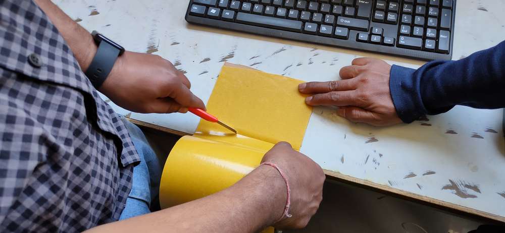
We were using FR1 type copper clad for milling the PCB. There is a thin copper layer for conduction and for the insulation, a phenolic paper
is used. It comes in variety of standard sizes so cut the clad according to your build area. To stick the copper clad on to the sacrificial
layer, we were using 3M double sided tape.
To test the precision of the endmills and the milling machine we were using this trace file:
http://academy.cba.mit.edu/classes/electronics_production/linetest.png
and this outline file:
http://academy.cba.mit.edu/classes/electronics_production/linetest.interior.png
Tracing means that the endmill will remove the unwanted copper layer from the surface. To trace the design, we were using 1/64 endmill,
1/64 means the diameter of the tip of the endmill is 1/64th of an inch.
Outline means cutting the PCB. For cuttin,we were using a 1/32 endmill. While cutting, the endmill penetrates through the copperclad
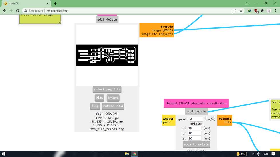
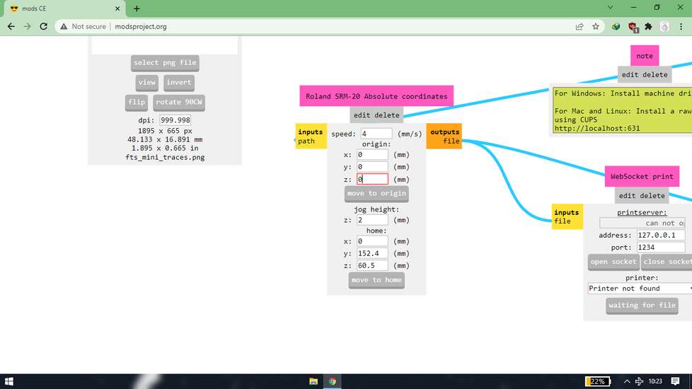
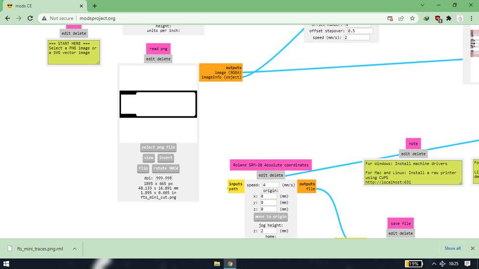
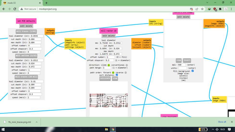
We were using mods community project to generate the toolpath/rml file and vpanel for communicating with the machine.Link for mods community
project: http://modsproject.org/
Upload the design file under the specific format tab
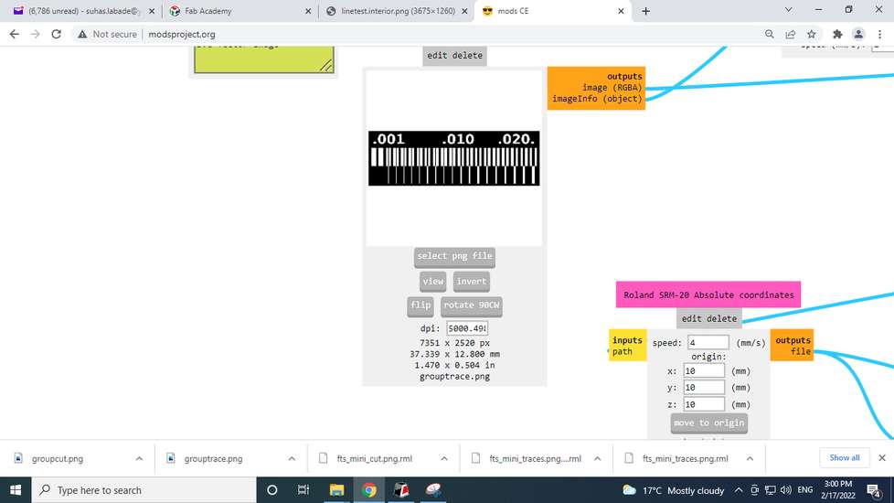
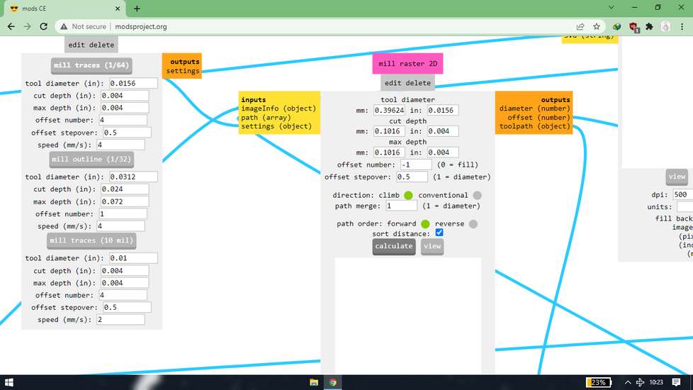
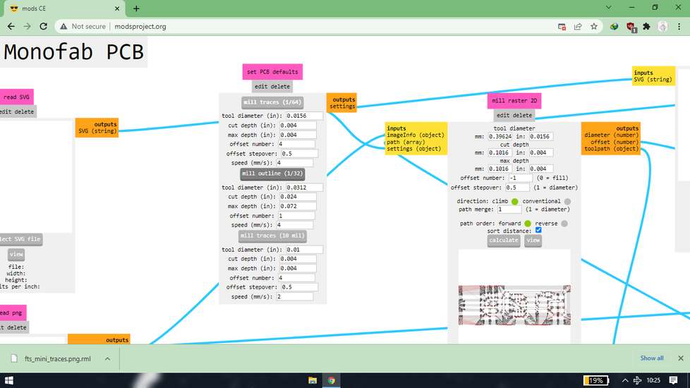
Under the “set pcb defaults” select mill traces (1/64)
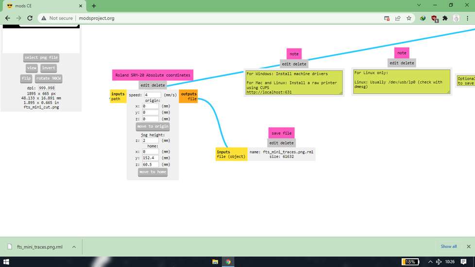
Under “roland srm-20 absolute coordinates” change the values of X,Y,Z to 0
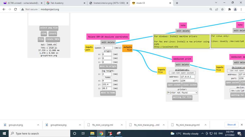
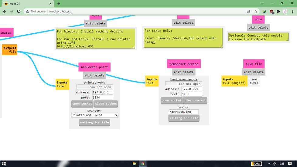
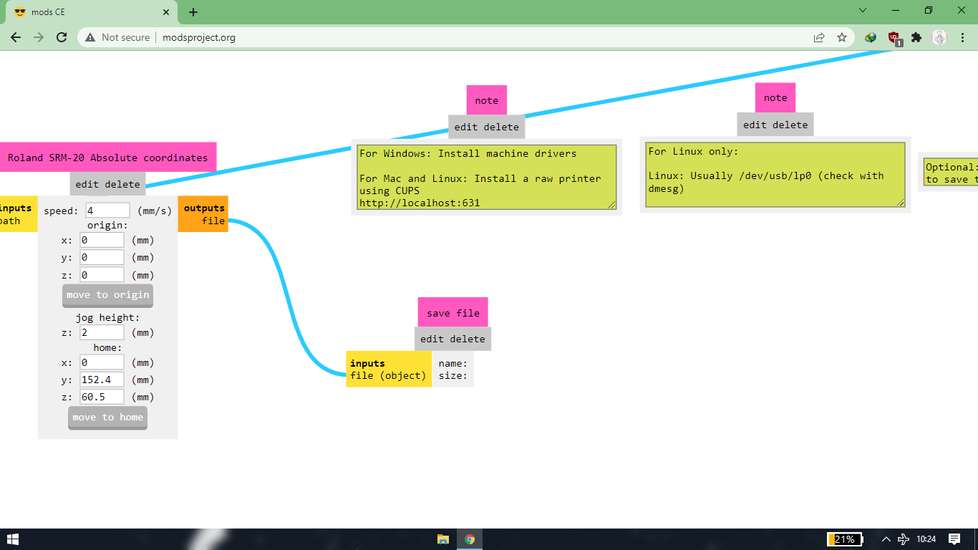
Since we just generate the toolpath, delete both of “websocket print” and connect the “output file” and “input file”


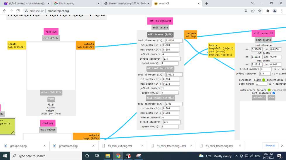
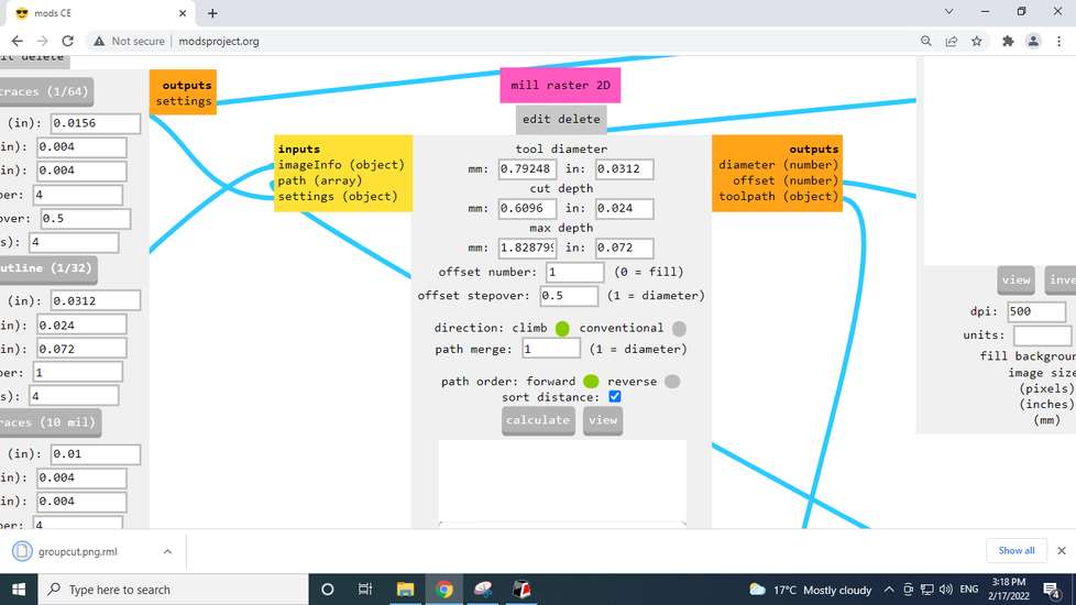
Under the “mill raster 2d” keep the “cut depth” and ”max depth” same, because we just want to remove the unwanted copper layer from the
surface. In the “offset number” set the value to -1 to completely remove the unwanted part. If you do not want to completely remove the
unwanted part, it is recommended to keep the offset number to 4. Higher the number, higher the amount of unwanted copper it will remove. For
tracing there are multiple HORIZONTAL passe
Repeat the same process for outline as you did for the trace, except select “mill outline 1/32” under “set PCB defaults” and depending upon
the thickness of your copper clad,change the “cut dept” and “max depth” under “mill raster 2d”. For cutting there are multiple VERTICAL
passes.
With the rml file for trace and outline ready, upload the rml file into the machine.
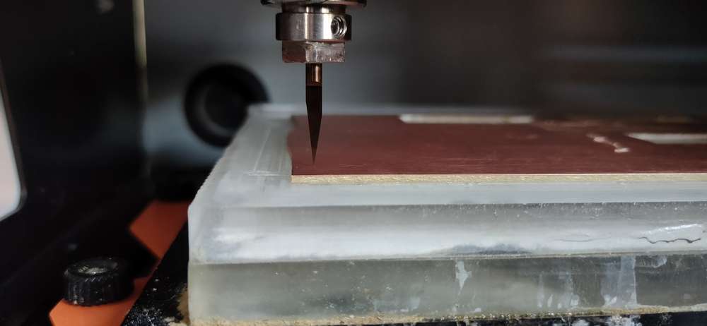
PCB Milling
<<<---TRACING--->>>
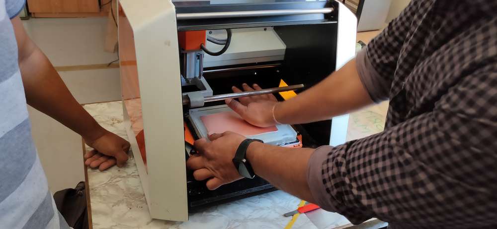
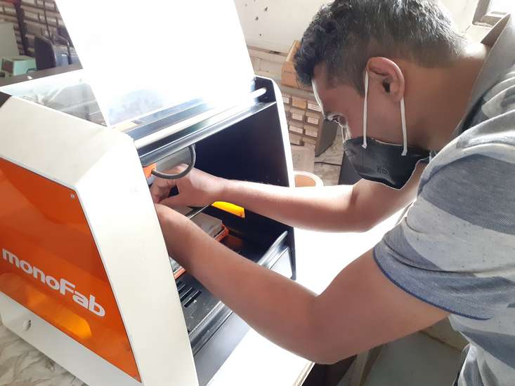
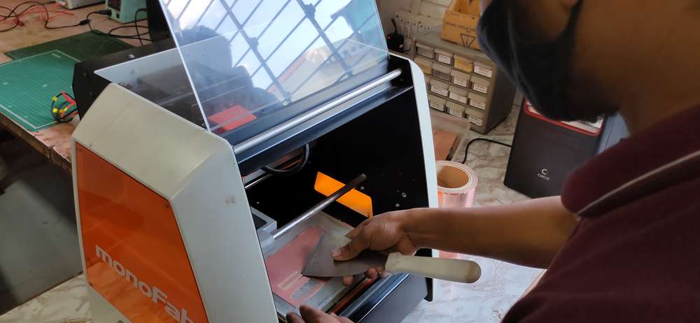
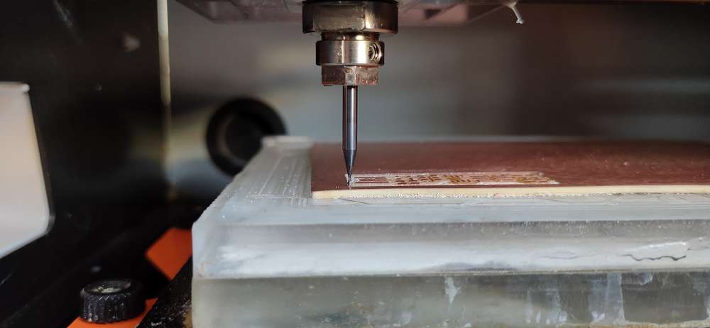
The first step for milling is to trace. Hold the endmill in one hand and with the allen key in the other hand Insert the 1/64 endmill into
the chuck, also known as collet.
Operate the position of axis with the help of vpanel. The interface of vpanel is quite self-explanatory
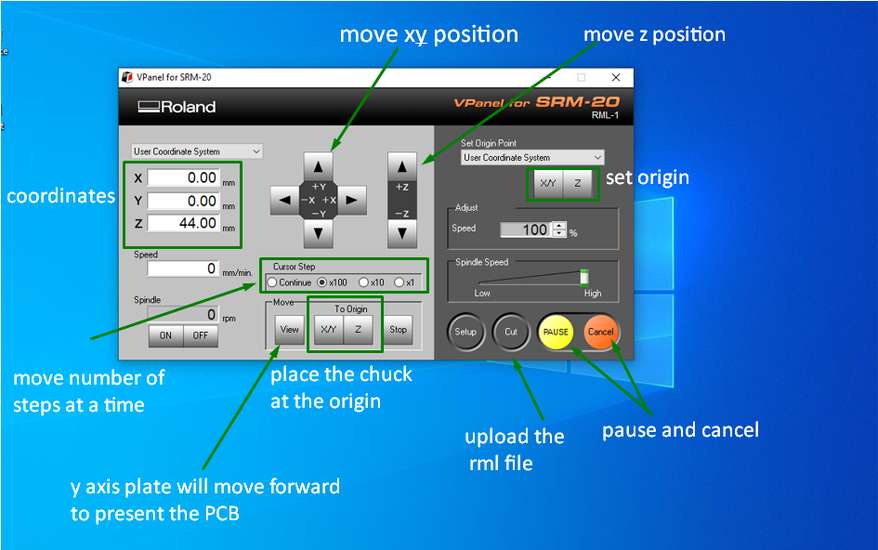
With the help of +x-x+y-y move the position of chuck on x and y axis. Once the position of chuck is positioned on x and y axis, set the origin
with “XY” button under set origin point.
With the help of +z-z buttons, move the chuck down to a point where the tip of the endmill is just above the PCB, but not touching the surface.
Now with one hand holding the endmill, loosen the chuck with other hand with the help of allen key, and carefully slide the endmill down so
that the tip of endmill touches the surface. Once the tip is touching the surface, tighten the chuck with allen key. This process of sliding
down the endmill is known as zeroing.
Remember that after the tip is touching the surface, see that the endmill should neither be too much inside the chuck, not it should be too
much outside the chuck, or else the tip of the endmill will break. We are already 4 endmills down in the inventory, may they rest in
peace!
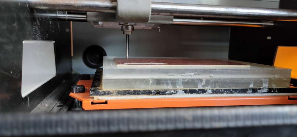
Set the origin of z axis by clicking on “Z” button under “set origin point”. From the “cut” button import the trace file and as soon as you
hit the “output” button, the machine will start tracing.
After the machine has completed tracing, remove the endmill from the chuck and thoroughly clean the debris from the machine,
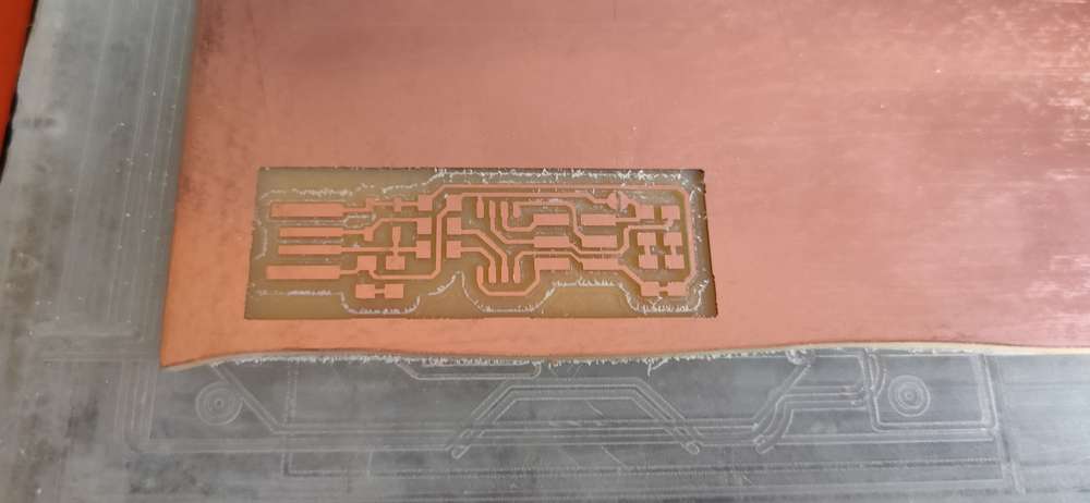
Here is the result of the trace,
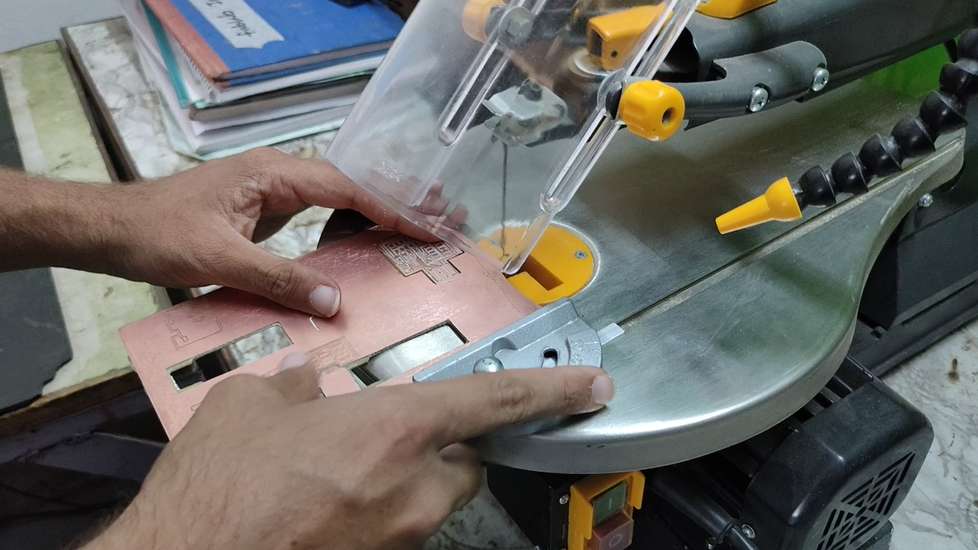
<<<---CUTTING--->>>
Insert the 1/32 endmill and place the endmill at the x and y origin. To do that click on “XY” button under “to
origin”. Remember that if you accidentally click on “XY” button under “set origin point” you’ll loose the old origin of x and y. After the
endmill is positioned at x and y axis, repeat the process of zeroing just like you did it with the 1/64 endmill. AFter the tip of the
endmill is touching the surface, set the new origin of of z axis by clicking on “Z” button under “set origin point”
From the “cut” button import the outline part and click on “output”. AFter the cutting is done, clean the debris from the machine and if the
PCB doesn't come right off, remove it with the help of spatula
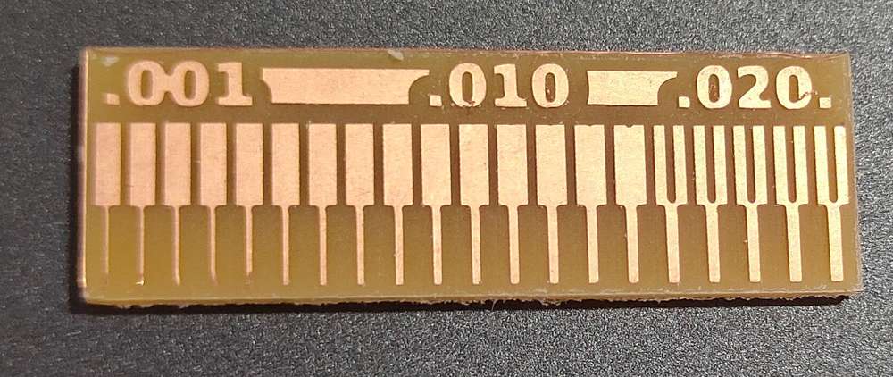
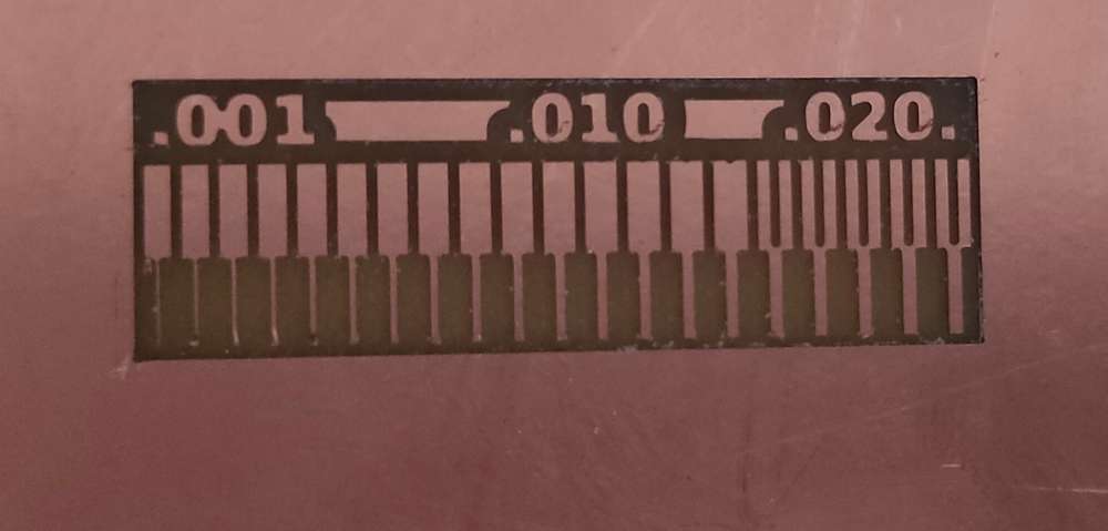
The reason behind milling this PCB is that we now know the strength and presion capacity of the machine as well as the 1/64 endmill. By
milling this PCB, we know that we can design the trace width of even 0.001 inch and it will do the job, with the risk of accidentally
removing the trace. For the trace gap, since the diameter of endmill tip is 0.0156 inch we cannot give design the PCB where the gap between
two traces is less than 0.0156 inches or else the machine will just ignore it and won’t trace it. You can see that in the photo above.
Individual assignment
In the individual assignment we were suppose to mill the PCB in milling machine, stuff the PCB with components and program
it to make it a In-System programmer. By the end of this week, one must know how to mill a PCB using milling machine and how to solder surface
mount components. The designing of PCB layout and getting to know the properties of all the input and output components will come in later
week in this course.
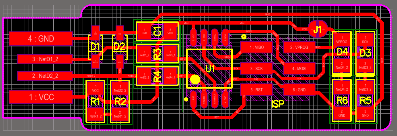
Generating toolpath
For the milling we need to apply the same principle we learned in the group assignment. From the available ISP design, I was using Brian's
FabTinyISP.
link for FabTinyISP: http://fab.cba.mit.edu/classes/863.16/doc/projects/ftsmin/index.html
Before jumping onto the machine, I generated the toolpath/rml file of tracing and outline
I selected “mill traces 1/64” under set “PCB defaults” and under “mill raster 2d” I set the offset as -1 since i wanted to remove all the
unwanted part(unwanted=things that is not white) and apart from offset I kept the values under “mill raster 2d” as it is.
I set the coordinates of X Y Z as 0 under “Roland srm-20 absolute coordinates”
Since i just wanted to generate the toolpath from the mods community project, I deleted both of the “websocket print” and connected the
“output file” and “input file”
Click on “calculate” under “mill raster 2d” to download the rml file
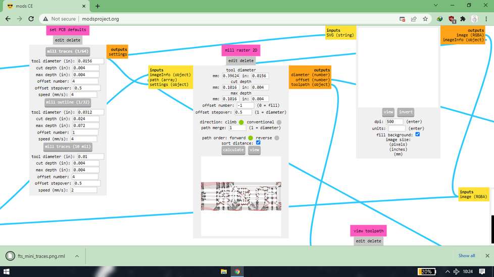
I repeated the same process for the generating the toolpath for outline except I selected “mil outline 1/32” under ‘set PCB defaults“ and
other than that I didn’t need to change any values. However, it is recommended to measure the thickness of your copper clad and set the “cut
depth”and ”max depth” accordingly under “mill rater 2D”. The thickness of the FR1 type copper clad we were using was 1.7mm so we kept the
default “max depth” as it is.
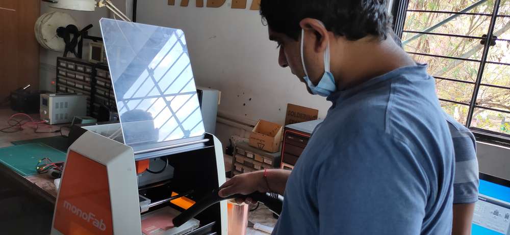
PCB Milling
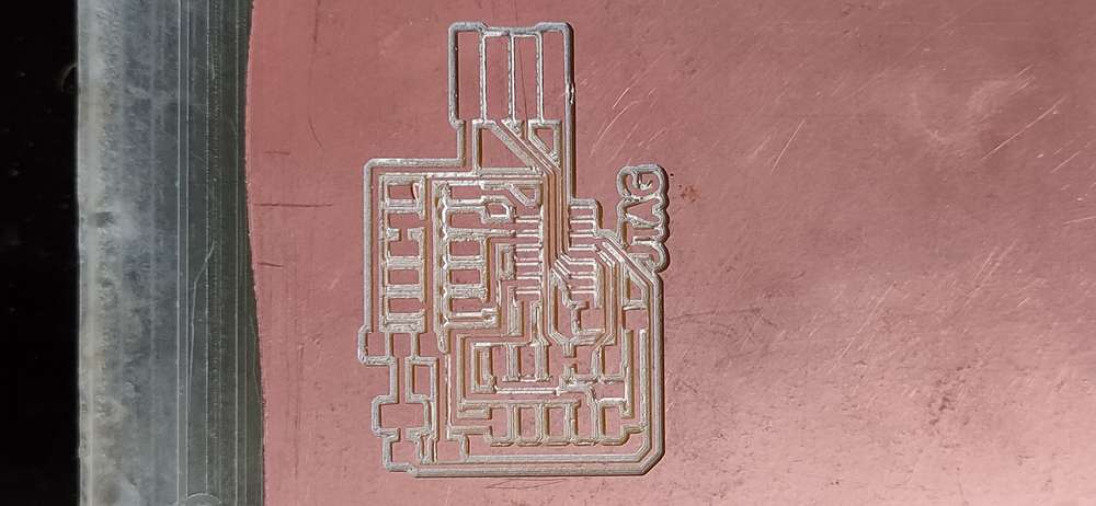
With both the rml files ready, i started the process of milling. First step is tracing.
<<<---TRACING--->>>
Stick the copper clad onto the sacrificial layer with the help of 3M double sided tape
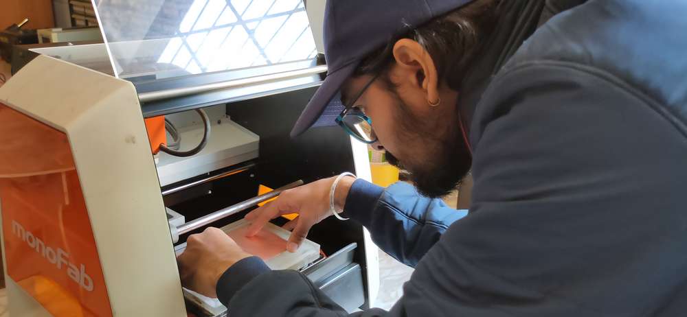
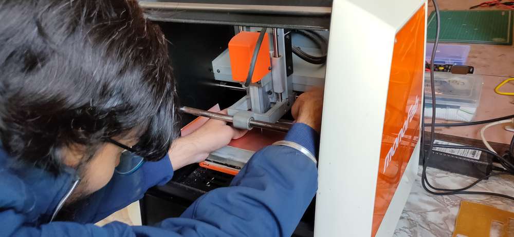
Insert the 1/64 endmill into the chuck. Hold endmill in hand and with the help of allen key, tighten the chuck with the other hand
Position the X and Y axis to your desired place by using vpanel.
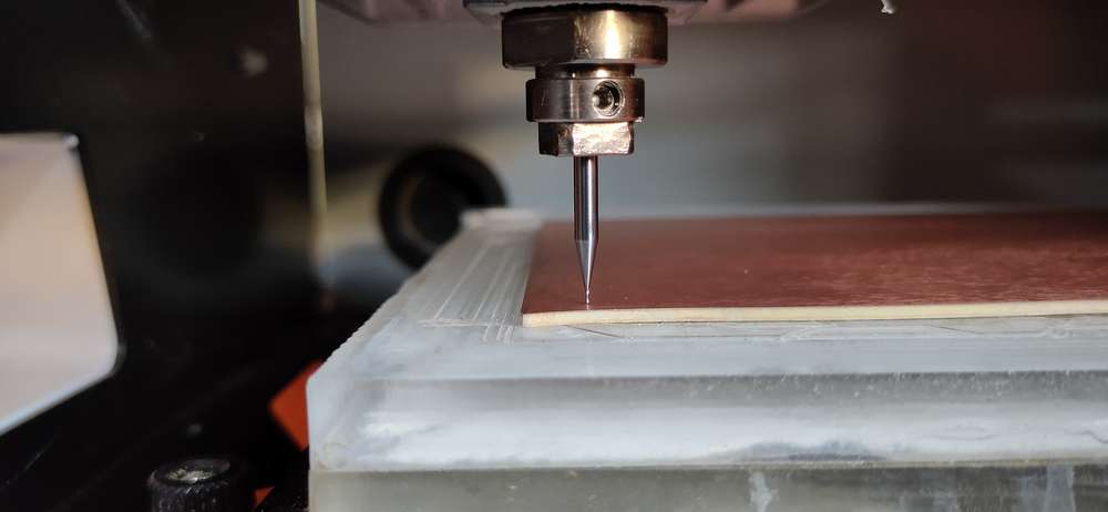
Lower the Z axis to a point where the the tip of endmill is just above the PCB but not touching the surface.
Then holding the endmil in one hand, loosen the chuck and slide down the endmill so that the tip of the endmill is touching the surface of
PCB and then tighten the chuck again. This process of sliding down the endmill is called zeroing. After the endmill is touching the surface of
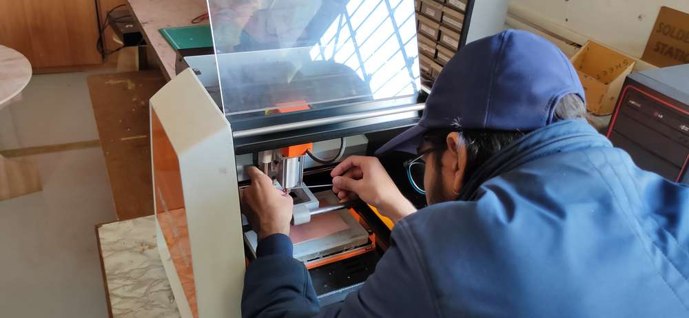
PCB, make sure that the endmill is neither too much inside
the chuck nor it is too much outside the chuck, or else the tip of the endmill will break. 4 of the 7 students had broken their mills, 2 of
which were broken due to the endmill inserted too much into the chuck or kept outside the chuck too much.
Set the origin for X,Y and Z axis from the vpanel. From the “cut” tab, select the trace file and click on “output” and the machine will start
milling,
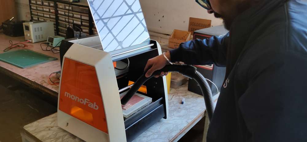
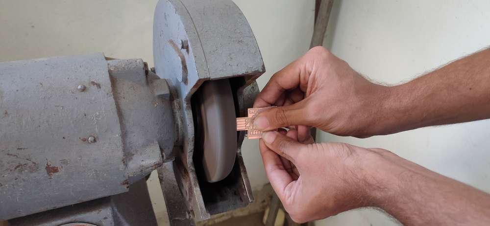
After the tracing is complete, there will be debris of copper and insulation onto the PCB and inside the machine, clean it thoroughly after
removing the endmill from the chuck
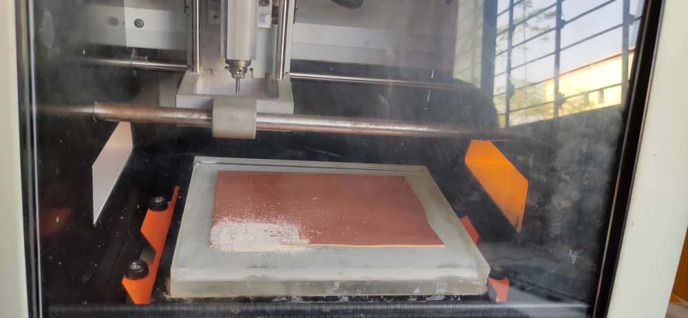
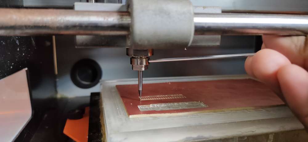
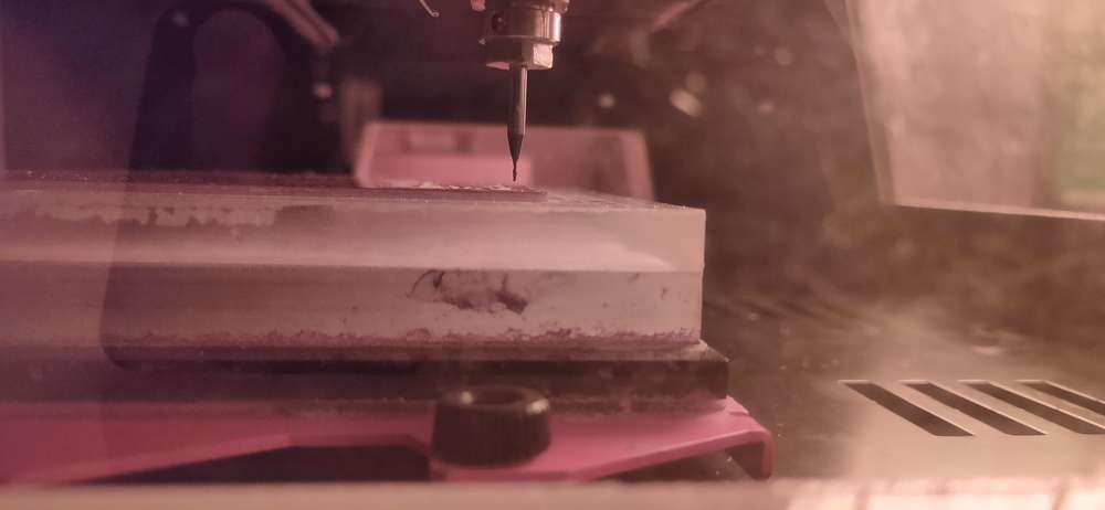
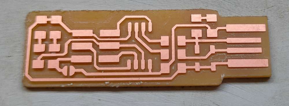
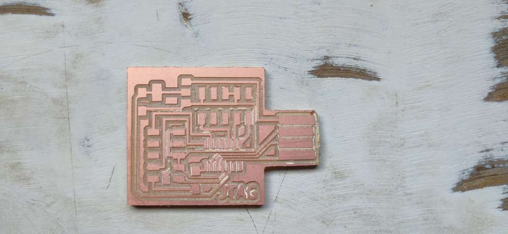
Here is the outcome of tracing
<<<---CUTTING--->>>
Now comes the cutting part,
Insert the 1/32 endmill. Position the X and Y axis to it’s origin and repeat the zeroing process, just like you did it with 1/64 endmill.
AFter the tip is touching the surface, do not forget to set the new origin. Be very careful using vpanel, do not accidentally click on “XY”
or “Z” button under the “to origin” instead of “XY” or “Z” under “set origin point”.
Inside the “cut” button, add the outline file and click on “output”
Again,there will be debris from cutting the PCB, so remove the endmill from the chuck and thoroughly clean the machine.
Here is the outcome
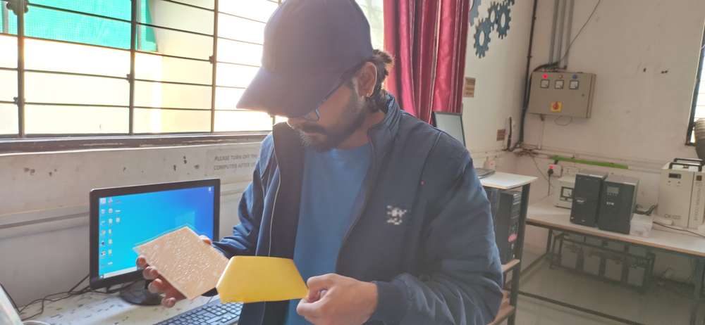
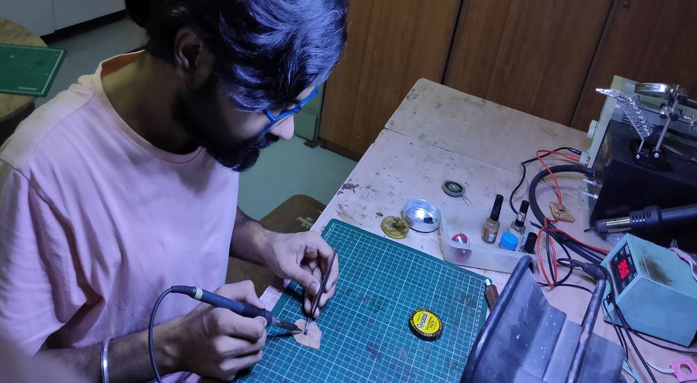
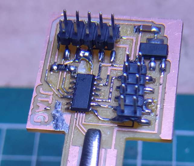
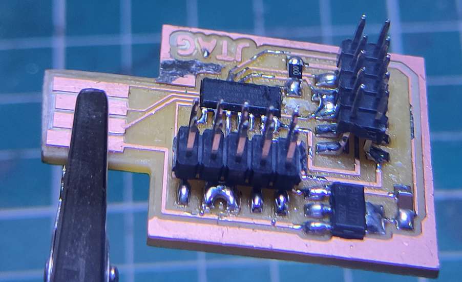
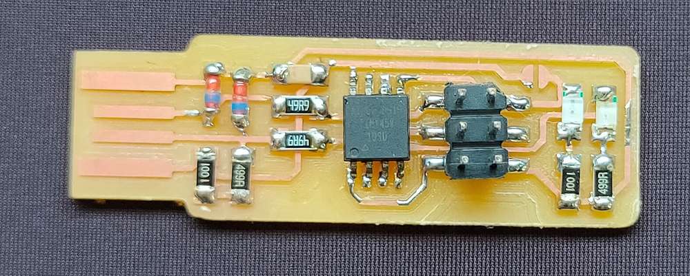
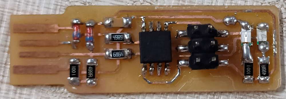
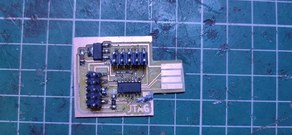
Soldering
Once the milling was done, I had to mount the components onto the PCB by soldering them. I had solder the through hole components onto zero
PCB before, but soldering these tiny surface mount components was my first time experience.
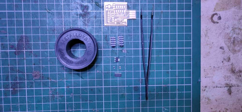
These were the components we were suppose to solder,
- 1x ATtiny45 or ATtiny85
- 2x 1kΩ resistors
- 2x 499Ω resistors
- 2x 49Ω resistors
- 2x 3.3v zener diodes
- 1x red LED
- 1x green LED
- 1x 100nF capacitor
- 1x 2x3 pin header
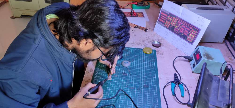
And here is the layout of PCB
http://fab.cba.mit.edu/classes/863.16/doc/projects/ftsmin/pcb_full.png
You'll find all the file and details of Brian's FabTinyISP here: http://fab.cba.mit.edu/classes/863.16/doc/projects/ftsmin/index.html
Here is how our workstation looks like,
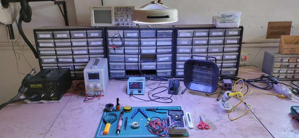
Here are all the tools required during the process of soldering
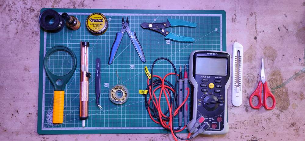
Startng from the top left, the names of the tools are,
Solder wire, liquid flux, paste flux, wire cutter, wire stripper, magnifying glass, de-soldering pump, tweezer, solder wick, multimeter, cutter
and scissor.
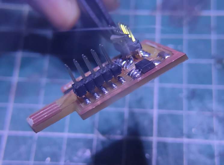
Here is how I soldered the surface mount components,
Apply the liquid flux over the PCB and wait for a few seconds to let the flux dry
With the help of tweezers, pick the component and place it over the trace. The components should be properly aligned on the trace or else it
will be hard to solder on one side of the component. Once the components is placed onto the PCB, hold the component down with the help of
tweezers so that when you solder it, the component doesn't slide from the trace
Clean the tip of the soldering gun(for soldering the surface mount components, use the soldering gun whose tip is very thin or else it will be
very difficult to solder the components and you might accidentally damage the component if too much heat is transferred to the component)
with the help of brass or stainless steel wool so it looks shiny. If there is old solder clogged onto the tip, it won't heat the solder wire
and it might damage the component of PCB if you contact the tip of solder gun with the component for too long. Once the tip is clean, touch
the solder wire onto the tip till there is a tiny blob(i'll use blob and melted solder interchangeably) onto the tip of the solder gun.
Holding the component down with the help of tweezers in one hand, contact the tip of the solder with the component and the melted solder will
automatically transfer from the tip to the component locking it onto the trace
Once one side of the component is locked, solder the other side of the component with solder wire in one hand and solder gun in other hand.
All you need to do is plade the tip of the solder gun very close to the component and melt the solder wire, once the wire starts melting,
contact the tip of of solder gun to the component and the melted solder should easily slide from the tip to the component and trace. Repeat
the same process on the other side where you had locked the component too, in case it was a dry solder.
This was the process for components like resistor or capacitor, having two ends. For the components like male header and IC(integrated circuit)
having 6-16 pins,instead of solder one side of the component first and then solder other side, what you can do is solder them diagonally
like first solder top left leg of IC and then solder bottom right, so that the IC will be locked properly. I highly recommend to watch Dua's
session on soldering. LInk for that: https://vimeo.com/669526883
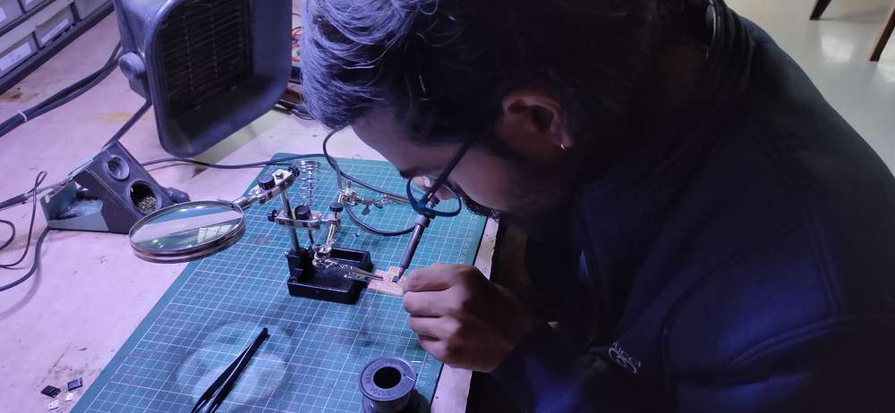
Note that after the components are soldered onto the PCB see to it if there is any acidental bridges between pins. Using the connectivity
function in multimeter will help you find if there is any short circuit or open circuit
Things that didn’t went smooth,
- The soldering tip was thin so it was easy to melt the solder from the components for de-soldering. However the solder wire we had was thick
in diameter compared to the tip so I was not able to melt it using the end of the tip. To melt the solder wire, I had to use the upper side if
the tip due to which the melted solder would never stick to the end of the tip but would slide upside the tip.
- Initially i was not cleaning the tip frequently due to which there were large blobs of solder onto the PCB, which i managed to remove using
de-soldering pump.
- I was accidentally making a solder bridge between the pins of IC. I did manage to de-solder them but soldering the IC with very tiny pins
was much harder compared to other components and turns out i had dry soldered the IC due to which I was getting “error 1” while programming
the ISP, more on that later.
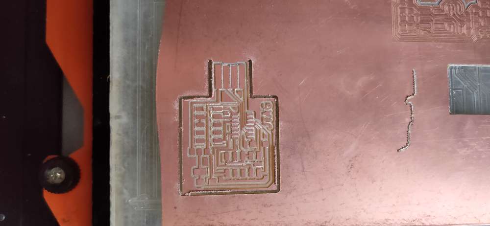
- While soldering the components onto the JTAG PCB, i wasn't paying attention to the layout of the PCB. In the JTAG's case there WAS a bridge
between the pins of IC. But when i was soldering them, i thought I accidentally bridged the two pins so firstly it was very difficult to
de-solder them, because i didn't know that there was a copper trace between the les, so with the help of scissor i completely removed the
solder and the trace was removed too. Then i realized that there is actually a trace between the pins, so i then bridge the pins by soldering
them
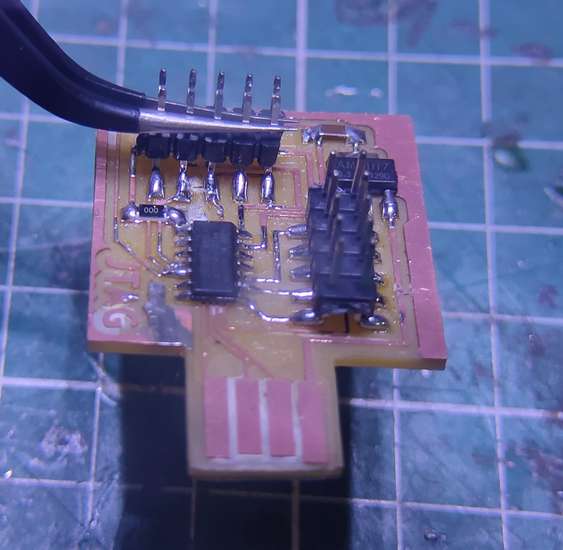
after i bridged the pins with solder,
- I accidentally removed a trace from the PCB, but managed to bridge the gap with soldering
Again, i wasn’t paying attention to the layout and description, so i forgot to bridge the two half circles, due to which, the led’s weren’t
working initially
software installation
Once the soldering was done, I had to test it if the ISP actually works. The goal was to make this ISP a programmer. The IC used in this ISP
is ATTiny45, after this ISP is converted into a programmer, we can use this to program other ISP’s
You will need to install a few softwares and follow some steps, for detailed description so to the Brian’s TinyISP link mentioned above.
I am using windows so i am mentioning windows’s steps
[1] Download git
Link: https://git-scm.com/downloads
I already had the git bash installed in program files
[2] Install the Atmel GNU Tolchain
Link: http://www.atmel.com/tools/atmelavrtoolchainforwindows.aspx
You will find the setup under “tools and resources” > “archives” > “AVR® and SAM MCU Downloads Archive”
I have this installed in program files
[3] Install GNU Make
Link: http://fab.cba.mit.edu/classes/863.16/doc/projects/ftsmin/make-3.81.exe
I have this installed in program files (x86)
[4] Install AVR dude
Link: http://fab.cba.mit.edu/classes/863.16/doc/projects/ftsmin/avrdude-win-64bit.zip
I have this installed in program files
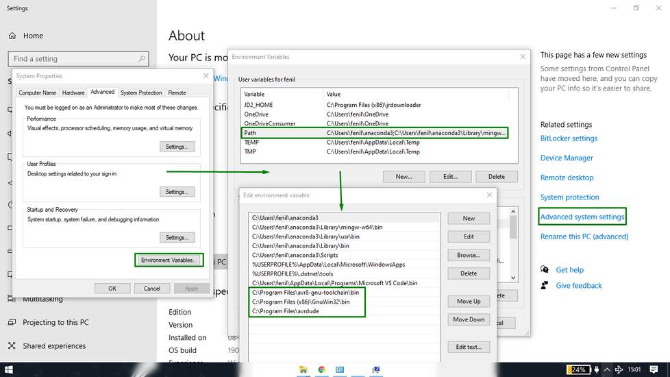
[5] Updating the path
So that windows will know where to locate this softwares when we type their name in command line.
Go to the control pannel > system and security > system.
Click on the “Advanced system settings” on the right hand side. A new window will pop up and under the “Advanced” tab click on
“environment variables”
Select “path” and click on edit.
Add these file location
- C:\Program Files\avr8-gnu-toolchain\bin
- C:\Program Files (x86)\GnuWin32\bin
- C:\Program Files\avrdude
[6] Install drivers
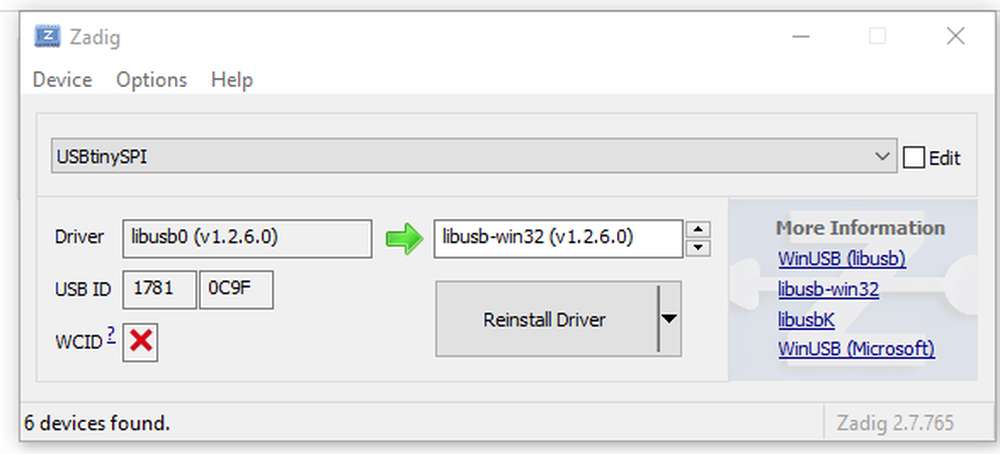
Install zadig
Link: https://zadig.akeo.ie/
Plug in a programmer ISP. Note that you are not suppose to plug in the ISP you just made.
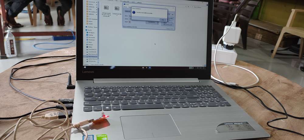
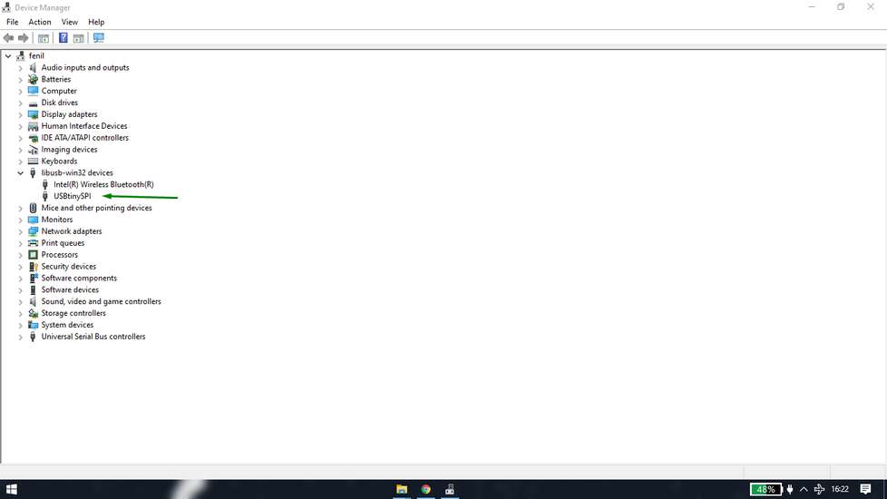
Open zadig and and select “USBTinyISP”. “Select libusb-win32(v1.2.6.0)”
If you cannot see the USBTinyISP, click on “list all devices” under “options”.
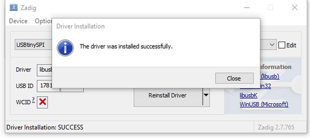
(for documentation purpose i used my ISP after it was made programmer and the driver was installed successfully,so this is another check to
see if the ISP i made works as a programmer or not.)
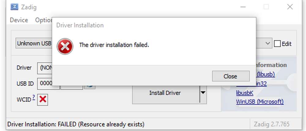
I made a mistake and plugged in my ISP(when it was not a programmer) so i was not able to install the driver.
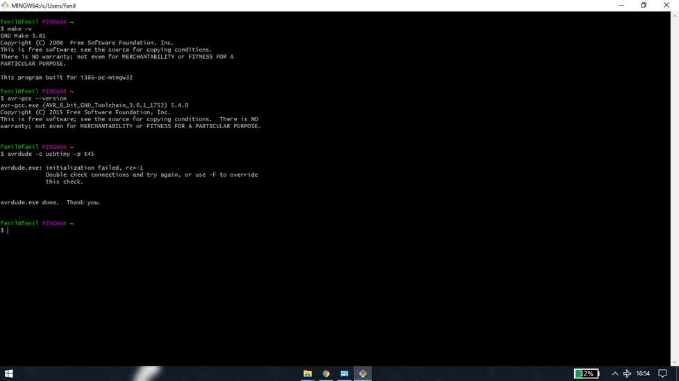
[7] Checking sanity
To see if the software we installed are working run these command in git bash one by one
make -v
avr-gcc --version
avrdude -c usbtiny -p t45
After running every command you should see the following messages. If not you made a mistake in giving path under “environment variables”
Programming
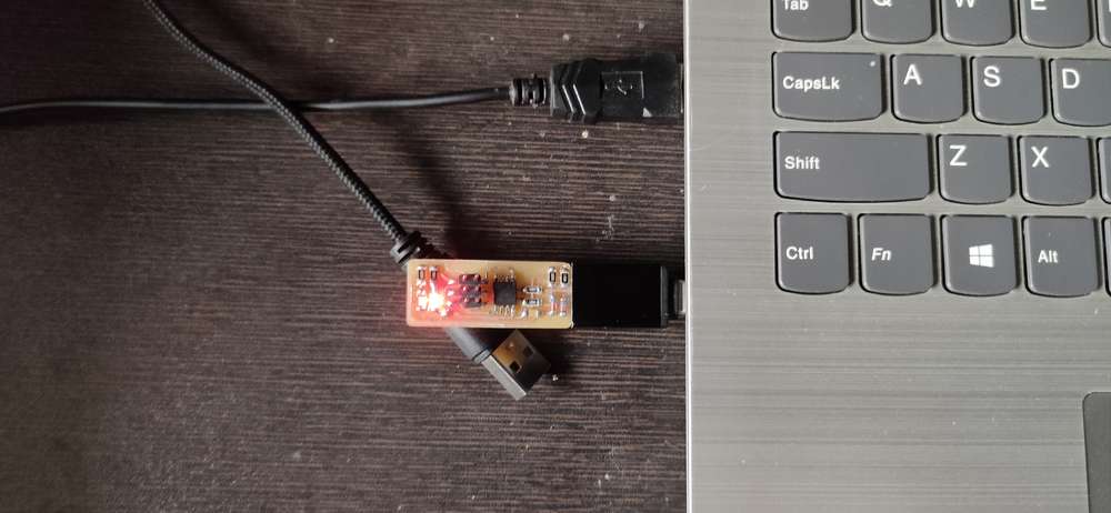
Plug in you ISP using data cable and you should see you ISP indicating green and red led
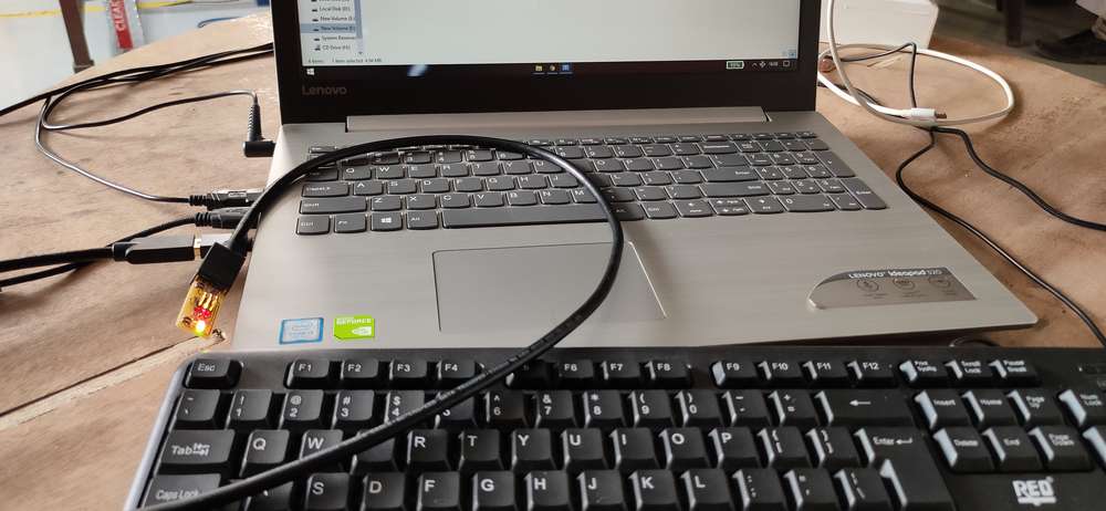
After checking, connect a programmer to the PC and connect your ISP to the programmer with the help of a connector. Check for the alignment of
connector before plugging in. For checking the alignment you can you multimeter.
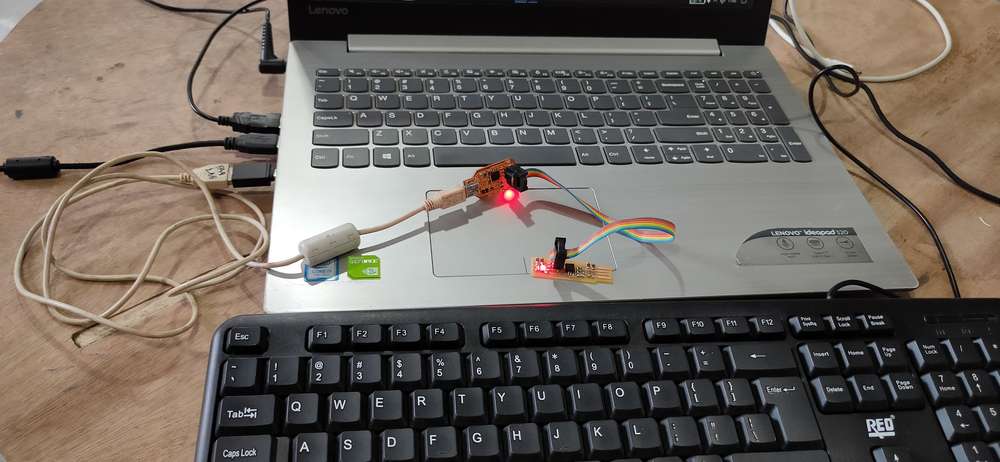
(the one on the upper side is the programmer and the one on the bottom is the ISP i made.)
Download the firmware and extract it. There will be make files there
Link: http://fab.cba.mit.edu/classes/863.16/doc/projects/ftsmin/fts_firmware_bdm_v1.zip
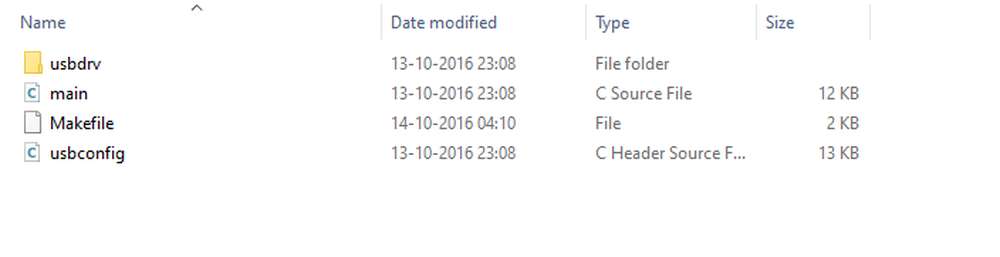
Open git bash and set the directory where you have extracted the firmware code. You can also go into that folder, right click and select
“git bash here” by doing that, git bash will automatically set the directory for you
Run these following commands
make
make flash
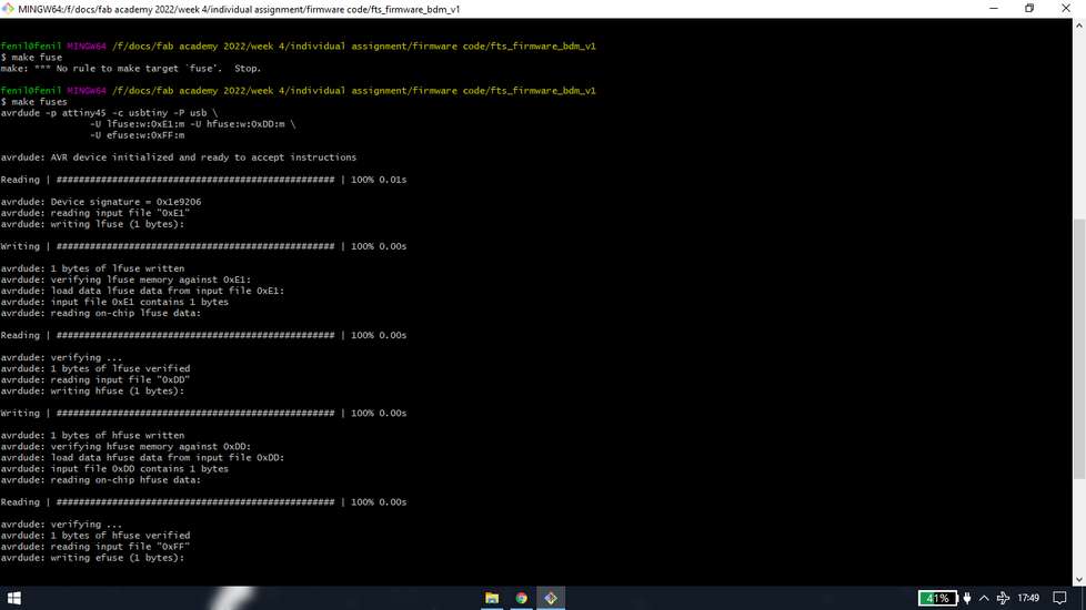
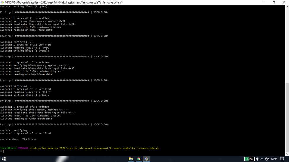
make fuses
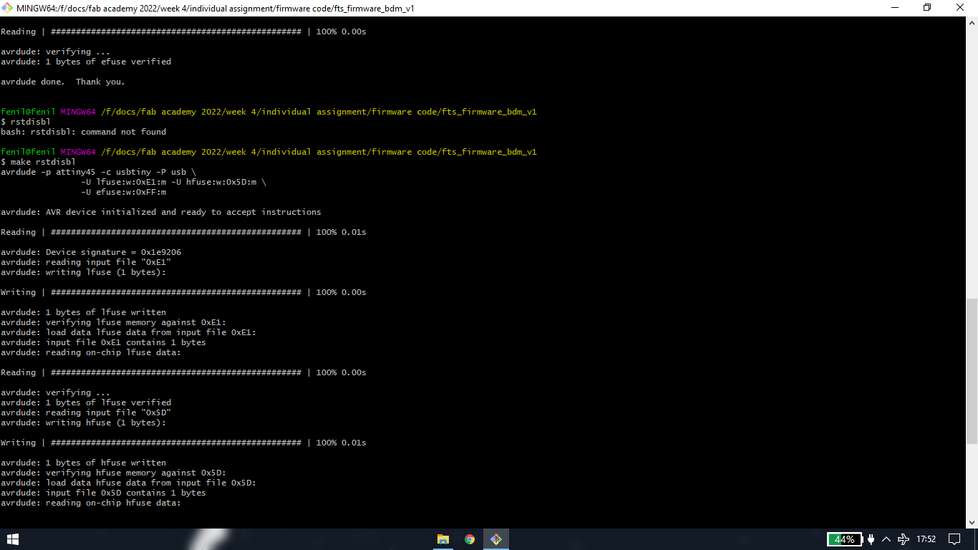
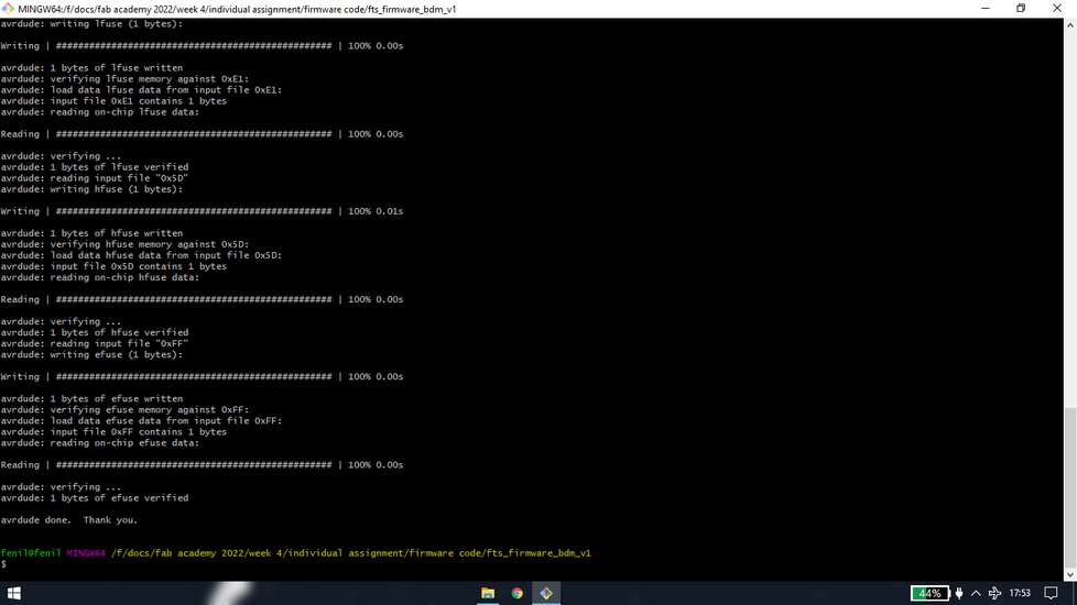
make rstdisbl
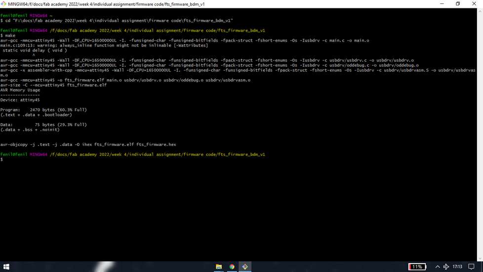
[1] make
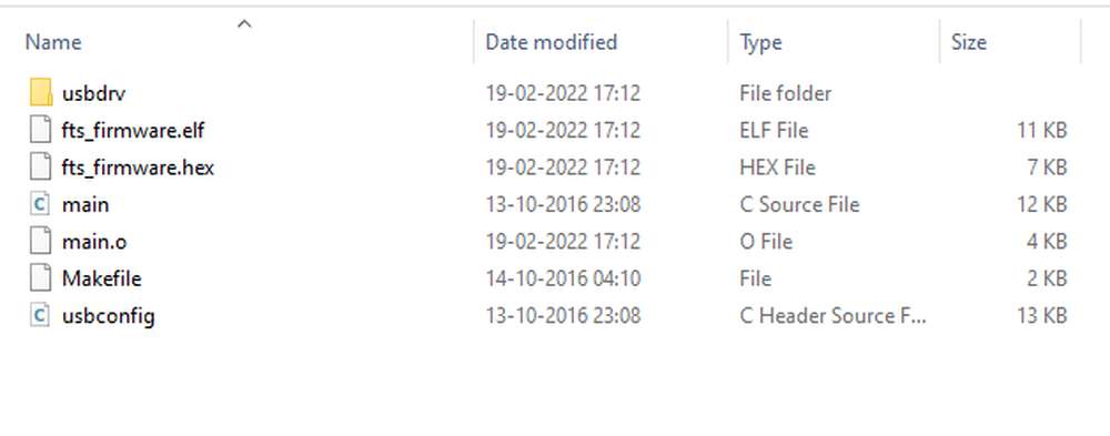
Type make and hit enter. This commad will conver make file into hex file. You will see the additional files after in the folder.
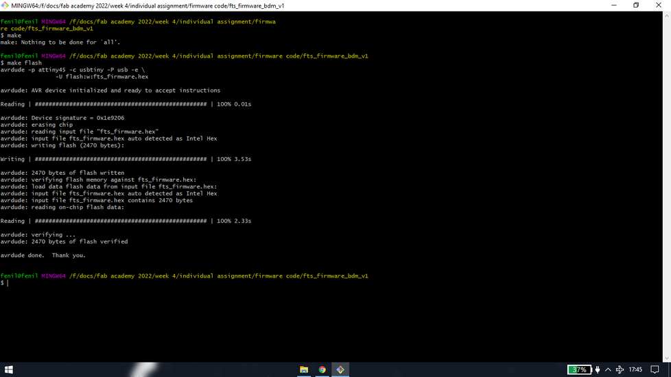
[2] make flash
This flashes/uploads the code into the ISP.
I ran the make flash command and was getting “error 1”
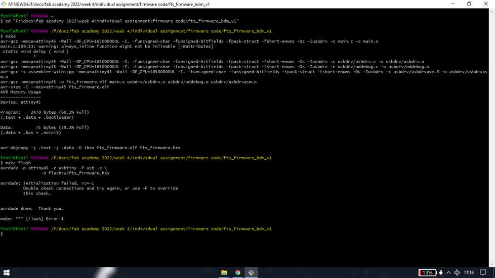
Turned out there was dry solder on the IC. M instructor helped me with soldering the IC and after that the command ran successful
[3] make fuse
This will set up all of the fuses except the one that disables the reset pin
[4] Reset disable
This will permanently make your ISP a programmer. You won’t be able to run another program in this IC
To check if your ISP is successfully made into programmer, connect that into your pc and the default name “USBTinyISP” wil show
Another way to check is to see the led. If it is constant red that means everything is fine
One another way to check is to reinstall the libusb driver using your ISP. If it is re-installed successfully that means your ISP is a
programmer. I have mentioned this method of checking above, under "instaling driver" part
One other obvious way to find out if everything is successful is to convert other ISP into a programmer using your ISP.
EXTRA CREDITS
JTAG
Learning Outcomes
This week I learned in brief about making a programmer and that if you make your custom board, you will need a programmer through which you program your custom board unlike Arduino boards where you don't need a another module to program. I also learned how to mill a printed circuit board with the SRM-20 machine and also get to know how precise the machine can be and it's limitations depending on the endmill configuration. Soldering the SMD components was something i did for the first time. As mentioned above, my local instructor had to help me re-solder/reflow the IC when i was getting the RC-1 error, so the soldering wasn't perfect however i was satisfied considering i was soldering the SMD components for the first time.
Drip Irritation by Fenil Chandarana is licensed under Attribution-NonCommercial-NoDerivatives 4.0 International![]()
![]()
![]()
![]()